
NXP MPC8360VVALFHA: A Comprehensive Technical Overview of the PowerQUICC II Pro Processor
The NXP MPC8360VVALFHA stands as a prominent member of the highly integrated PowerQUICC II Pro family of communications processors. Designed for a broad spectrum of embedded networking and telecommunications applications, this system-on-chip (SoC) combines high-performance processing with a rich set of integrated peripherals, making it a cornerstone for complex, connected systems.
At the heart of the MPC8360 lies a dual-core architecture that effectively separates control-plane and data-plane processing. The main processor core is based on the enhanced Power Architecture e300c3 core, a derivative of the PowerPC G2 series. This core, capable of operating at speeds up to 667 MHz, handles the control functions, running the operating system (such as Linux, VxWorks) and management protocols. Its integrated Harvard architecture and 32 KB L1 instruction and data caches ensure efficient execution of complex tasks.
Complementing the main core is the RISC-based Communications Processor Module (CPM). This secondary processor is dedicated to handling the data path, managing communication channels, and accelerating peripheral tasks, thereby offloading the main core. The CPM integrates two powerful 32-bit RISC controllers and supports a vast array of communication protocols, including Ethernet (10/100/1000 Mbps), ATM, HDLC, PCI, and USB 2.0. This offload architecture is critical for achieving high throughput without burdening the main CPU.
A key feature of the MPC8360 is its sophisticated memory subsystem. It includes a 256 KB L2 cache associated with the e300 core, significantly reducing latency and improving overall system performance. The processor supports a flexible memory controller capable of interfacing with various RAM types, including DDR1/DDR2 SDRAM, as well as NOR and NAND flash memory, providing designers with ample options for system design and scalability.
The integration level of the MPC8360VVALFHA is exceptional. Beyond the cores and memory controllers, it incorporates a plethora of standard interfaces:
A 32-bit PCI controller for expansion cards.
Dual triple-speed Ethernet controllers (TSECs) for Gigabit network connectivity.
A USB 2.0 OTG (On-The-Go) controller with integrated PHY.
Serial interfaces including UART, I2C, and SPI.
This high level of integration reduces the total component count on a board, leading to lower system cost, reduced power consumption, and increased reliability.
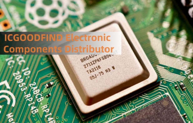
The device is offered in a 783-ball, 29x29 mm TBGA package, identified by the suffix 'VVALFHA' which specifies its performance grade, temperature range, and packaging details. It is engineered for extended temperature ranges, making it suitable for industrial environments.
Target applications for the MPC8360 are vast and include enterprise routers, switches, industrial control systems, network-attached storage (NAS) devices, and wireless infrastructure equipment like radio network controllers (RNCs).
ICGOODFIND: The NXP MPC8360VVALFHA is a highly integrated, dual-processor SoC that exemplifies the PowerQUICC II Pro's strength in embedded communications. Its blend of a high-performance e300 core, a dedicated communications processor (CPM), a robust memory subsystem, and extensive peripheral integration makes it a powerful and versatile solution for demanding networked applications.
Keywords: PowerQUICC II Pro, Communications Processor Module (CPM), Power Architecture e300 core, Integrated Peripherals, Embedded Networking.

